Project Overview
We are reinforcing our knowledge on our k-mapping skills, NAND gates, NOR gates, Circuit designing and Seven-Segment Displays. We needed to show all of our work when finding out our simplifications, because instead of boolean algebra, she spared us with k-mapping. From this she wanted to use our display of knowledge and use the NOR gates and NAND gates to make the circuit simpler. With this knowledge I was able to make a better working circuit design and less trouble shooting.
Truth Table
Below shows the truth table I designed so that I could come up with the circuit design I used to build this project. We need to convert the seven switches so we can be able to only use three switch's so that it is less when trying to light up the correct symbol.
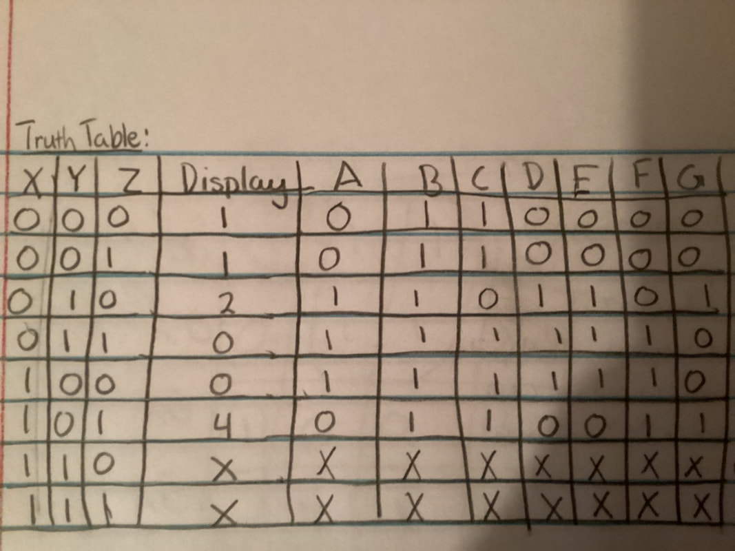
We have a through g columns on our truth table because we have seven segments of the display we need to control in order to get the correct symbol. Using that we are able to get the output we need when using our switches which are the x, y and z columns. In those columns we use regular truth table set up we are used to get the display with the seven-segment display. Through this we use a series of gates and get the output putting those switches through the circuit.
K-mapping and Simplified Logic
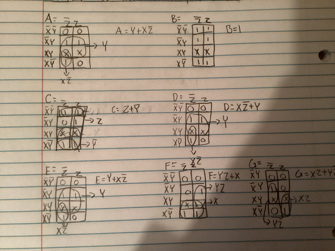
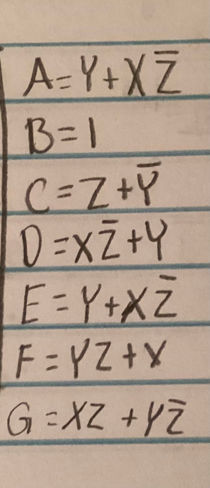
Above you see my process of k-mapping to get the output I needed to create the circuits. K-mapping starts with the seven-segment display in which one we need to be turned on. from there we take that information an put it in a k-map with the x, y and z to get the logic expression for the three switches. After getting the answer, the answer will come out in the sum of products form. We use grouping to be able to arrive at each of the expressions that I have above. Using groups of two and four. K-mapping is able to give the accurate answer faster and more efficiently if you group them right. I really didn't have that many expressions because some had the same expression or were just connected to power. Though for others it is so big because there is seven segments so u need an expression for each segment.
Multi Sim Implantation
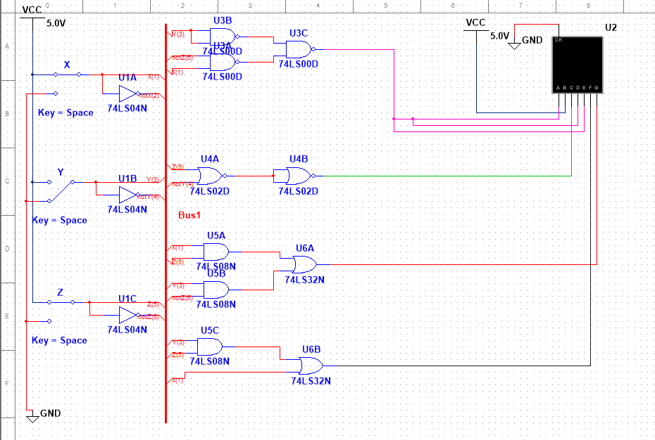
First I started with implementing all the components I would need because I knew from before when creating the circuits for each what I needed to implement. using a bus I was able to organize my components in a way I was able to read where each wire was going. From here I needed 3 Not gates, 3 Nand gates, two Nor gates, 3 And gates, and 2 Or gates. After Examining this information I can see that 1 chip for all five different gates.
We are implementing Nor and Nand gates in our circuit so that we can simplify the circuit. By using nor and nand gates in my circuit I was able to decrease the amount of gates I needed to use. This is important so that we have an efficiently working circuit. The more chips and process we use the more cost for manufacturing and materials and we do not want to spend more money. We want to spend less.
We are implementing Nor and Nand gates in our circuit so that we can simplify the circuit. By using nor and nand gates in my circuit I was able to decrease the amount of gates I needed to use. This is important so that we have an efficiently working circuit. The more chips and process we use the more cost for manufacturing and materials and we do not want to spend more money. We want to spend less.
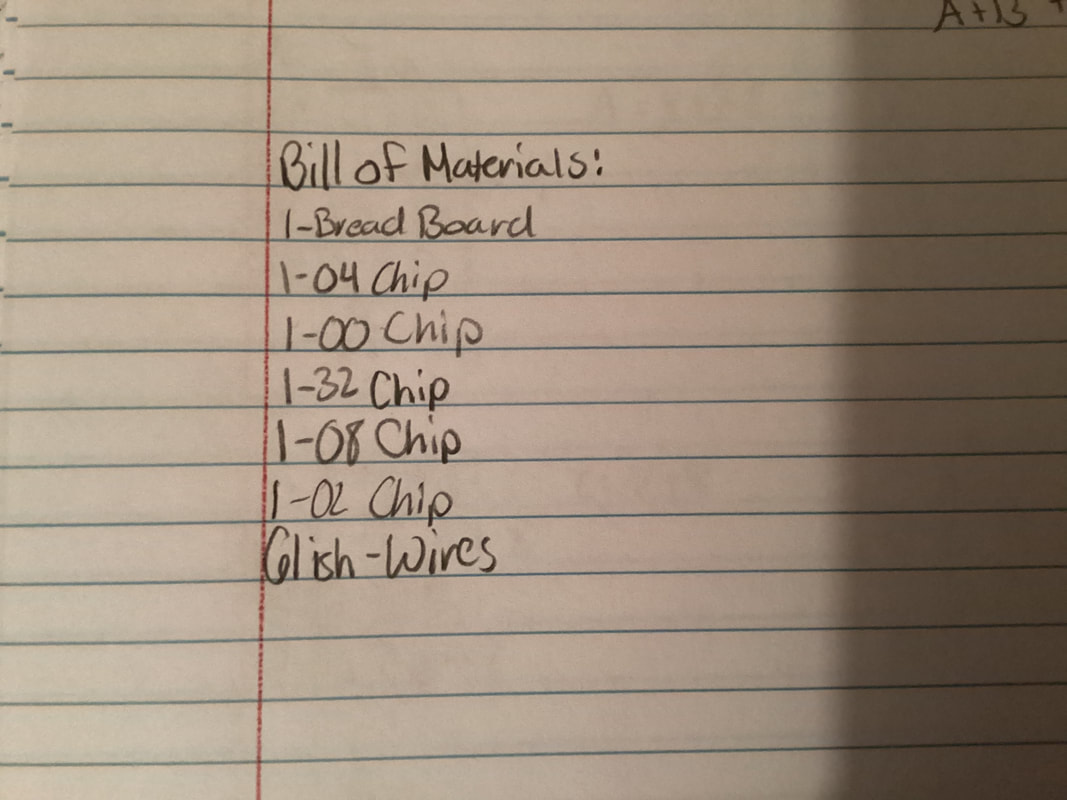
Bill of Materials
Below is the Bill of materials that contains how many components I used in my project. From this you can see that the most things I used was wires which is reasonable and that I only had to use 1 of each chip.
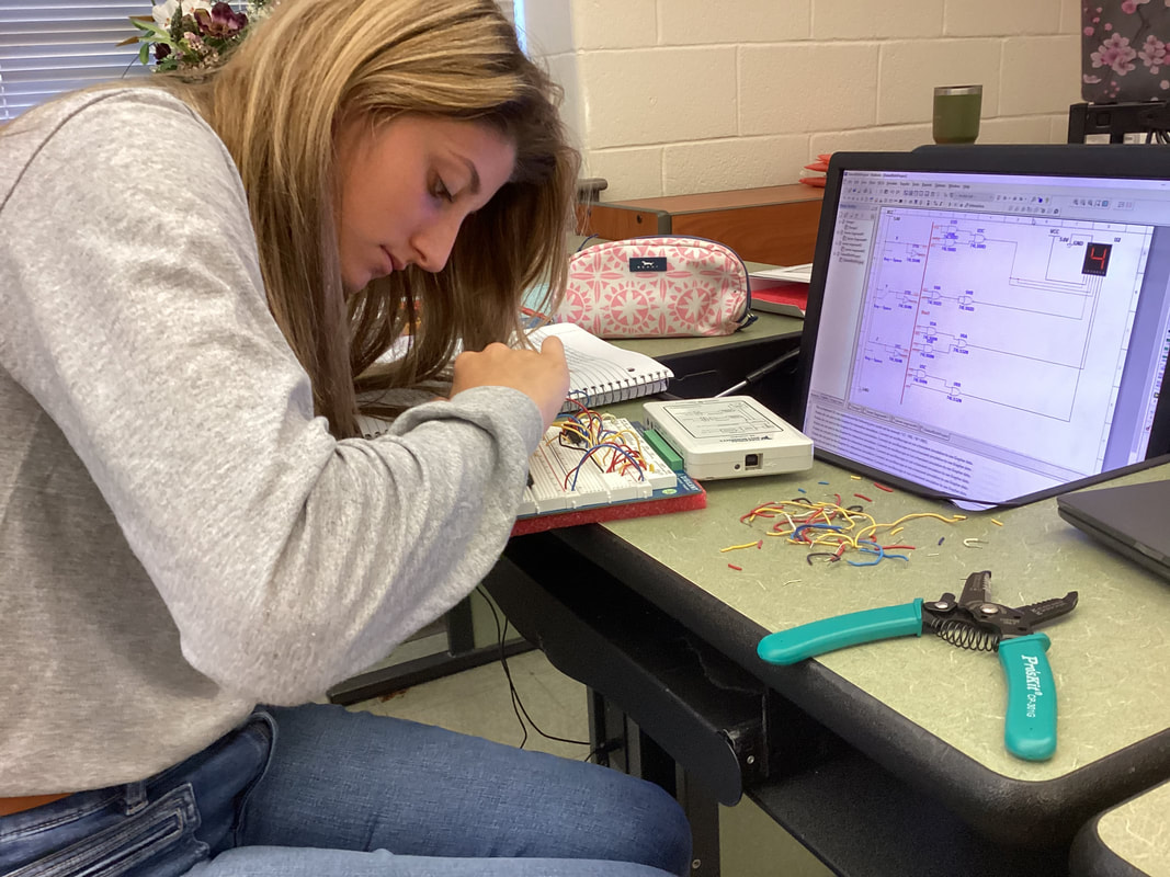
Bread-boarding
Here I am finishing up my circuit with building the last two circuits. Which are my g and f.
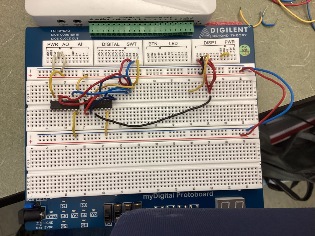
Here I have just completed the first circuit which is also a total of three circuits because they are all the same.
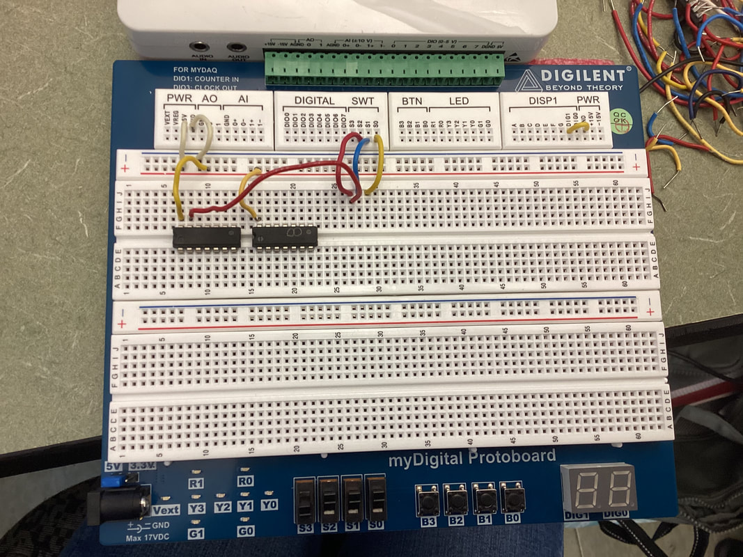
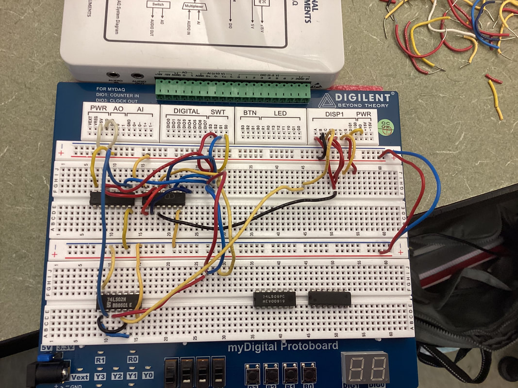
This is where I'm just starting to wire my circuit and connecting the switches so that I can create my first circuit. This also shows powering and grounding the board.
I have learned that I need to triple check everything so that my circuit is efficiently working and when troubleshooting making sure to check even the tiniest things. Something I made a mistake on is having my power and ground wrong when grounding and powering the chips. then a big thing I missed was accidently having one of my chips backwards. Which was pulling power and making my whole circuit go off wack. additionally with that chip being backwards that chip had a bent pin making that chip not work correctly. So when building I defiantly need to take a closer look at the smaller things on my circuits.
Conclusion
I learned that in this project i need to look closer and be more efficient when bread-boarding. That looking closely always helps in the end goal. Next time I would definitely take a step back and take different perspectives of what others see in my project to see if they see something wrong when trouble shooting because a new set of eyes always helps. I really don’t have any questions everything I was confused about was enlightened to me during the project. As in the Nor gates the chip swaps the gates and I was able to learn through out my project.
